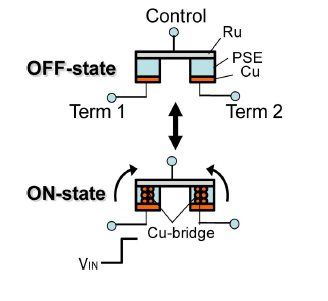
NanoBridge (NB) is a new switch device used with semiconductor devices to partially replace conventional semiconductor memory and switch. NB is composed of polymer solid-electrolyte (PSE) sandwiched between inert Ru and active Cu electrodes. When a positive voltage is applied to the Cu electrode, the Cu atoms are ionized from the Cu electrode and make a Cu bridge between the electrodes, resulting in a low-resistive ON-state. Contrary, a negative voltage is applied, the Cu bridge is ruptured to the Cu electrode, turning to a high-resistive OFF-state. The both resistive state is repeatable and stable (nonvolatiity). In addition. NB has lower input capacitance as compared to the conventional CMOS switch and higher off/on resistance ratio. Thus, NBs are applicable to the switch for routing signals and memory for information storage.
NanoBridgeは半導体スイッチと半導体メモリの両者を同時に置き換えることができる新しい不揮発スイッチです。NanoBridgeは、ポリマー固体電解質(Polymer solid-electrolyte: PSE)を不活性電極であるルテニウム(Ru)と活性電極である銅(Cu)で挟んだ構造からなります。銅電極側に正の電圧を印加すると電極の銅がイオン化し、ポリマー固体電解質内を移動して両電極間に架橋を形成します。その結果、NanoBridgeは高抵抗(オフ)状態から低抵抗(オン)状態へ遷移します。逆に、銅電極側に負の電圧を印加すると架橋を形成する銅原子が銅電極側に回収され、高抵抗状態へと遷移します。NanoBridgeは繰り返し書き換えが可能で、かつ、各オン・オフ状態を維持するための電力を必要としません(不揮発性)。また、半導体スイッチに比べて負荷容量が小さく(半導体スイッチの10分の1程度)、オン・オフ抵抗差が高い(500Ωと1GΩ)などの電気的特性を備えています。そのため、論理信号を切り替えるためのスイッチと回路情報を保持するためのメモリとして用いることができます。
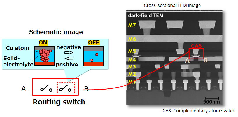
Schematic image of operation and TEM image of NanoBridge
The thickness of the Cu bridge in the NB is expected around sub-10nm, which is applicable to further scaled logic CMOS design rules. Two NBs are connected in series with opposite direction for routing switch in FPGA, in which the “control” transistor is connected between the two NBs (1T2R). To transfer signals, the two NBs have the same resistive state. In the off-state, operation voltage is applied to the switch, where the voltage is divided in two. The improvement of the OFF state lifetime is explained. (1) When logic operation voltage Vop is applied between Term1 and Term2, the NBs divide Vop; hence, ∼ Vop/2 is applied to each NB. The decreased stress voltage results in higher OFF-state reliability. (2) When the OFF-resistance of the NB biased to “turn-on” direction starts to degrade, the other NB biased to “turn-off” balances the voltage owing to its high resistance. The NB biased to “turn-off” maintains the OFF-state until breakdown. Based on the concept above, the OFF-state lifetime is kept long in the CAS (complementary atom switch). For nonvolatile memory application, one transistor one NB structure (1T1R) is used.
銅架橋の太さは、数nmと推定されていて、より集積化が進んだデザインルールにおいても回路に組み込むことが可能です。NanoBridge-FPGA(NBFPGA)で用いる際には、2つのNanoBridgeを向かい合わせに接続し、ルテニウム電極側の中間端子に書き込み制御用のトランジスタをつなげた構造とします。信号切り替えには、2つのNanoBridgeをともにオンまたはオフ状態とします。オフ状態のスイッチに動作電圧が印加されると、2つのNanoBridge間でその電圧ストレスが分配されます。これに加えて、電圧ストレスの方向に対して2つのNanoBridgeのどちらか一方は、必ずオンからオフへプログラムする電圧方向になるように配置しているため、オフ状態の信頼性を相補的に高めることができます。この相補型NanoBridgeによって、電圧ストレス下の保持寿命は飛躍的に向上しています。また、本構造では、中間ノードを介して個々のNanoBridgeをプログラムするため、オフ信頼性とトレードオフ関係にあるプログラム電圧を低く抑えられます。不揮発メモリとして用いる際には、1つのNnoBridgeに対して1つの選択トランジスタをつなげた構造とします。
Schematic image of the OFF-state lifetime improvement of the NB for routing swtich
NanoBridge has the following characteristics;
NanoBridgeは、以下の特徴を有します。
Low power consumption: Replacing the semiconductor memory and routing switch by NBs, area of logic block can be reduced and low power consumption can be realized.
低消費電力:半導体メモリや信号線を切り替える半導体スイッチをNanoBridgeで置き換えることで、論理ブロックの面積を小さくでき、低消費電力化が実現できます。
Low cost: Only two additional masks are required to add NBS for standard CMOS process without any changes of PDK. No dry-etching process is needed for integrate the Cu electrode since Cu interconnect itself is used as the Cu source.
低コスト:NanoBridgeは、標準ロジックCMOSの製造プロセスにマスクを2枚追加することで製造することができます。ロジックCMOS・多層配線製造に対応した製造プロセスであるため、CMOSや配線パラメータの変動なくNanoBridgeを多層配線層内に形成することができます。NanoBridgeの銅電極には銅配線を用いる構造としているため、銅電極のドライエッチングが不要となる特徴も有します。
Rad-hard: NanaBridge has high resistance against radiation. Usually, SRAM having electron charge is used for memory. However, the charge-based memory is very weak against the radiation from space and state flip is frequently occurred. NBs having a physical connection of the bridge give very high resistance for the radiation (rad-hard)
放射線耐性: NanoBridgeは、放射線への耐性も備えています。半導体で一般的に用いられてるSRAM(Static Random Access Memory)は、電荷数の違いによって、オンとオフ状態を維持しています。高いエネルギーの放射線が入射すると、半導体基板中で放射線がシリコン原子と衝突して電荷が発生するため、これらがSRAM上の電荷を乱し、状態を反転する不具合を発生させます。NanoBridgeは物理的な銅架橋の有無によってオンとオフ状態を実現していることから、放射線により発生する電荷によって状態が変化することはありません。
Temperature stability: NBs have high temperature stability as compared to CMOS transistor. Lower static power consumption of NBFPGA is confirmed to the conventional SRAM-based FPGA at the temperature range from -50oC to 150oC.
温度耐性: 高温下では、トランジスタのオフ電流が温度に対して指数関数的に変化するのに対して、NanoBridgeのオフ抵抗の変化は小さく抑えられます。そのため、環境温度が高い場合においてもSRAM-FPGAと比較して、待機電力の増大が少ないという利点があります。また、NanoBridge- FPGAは-50℃から150℃まで正常に動作することを確認しています。
※本ページの記載は、PUBLICATIONSに記載の解説記事から引用しています。
APPLICATION
NanoBridge FPGA
NanoBridge NVM