Field-Programmable Gate Arrays (FPGAs) are integrated circuits that allow users to configure internal circuitry (hardware) to build processing blocks and dataflows directly on the chip, tailored to specific applications. Like CPUs, FPGAs offer a high degree of flexibility. Since they perform information processing using non-von Neumann hard-wired logic (wired logic), they are more power-efficient than von Neumann-type processors. As a result, they are expected to play an increasingly important role in edge computing.
Challenges:
Although FPGAs are general-purpose devices and do not require users to develop custom integrated circuits, they incorporate a large number of semiconductor switches for changing circuit configurations and SRAMs to store those configurations.
This leads to increased circuit area and standby power consumption. Moreover, since SRAM requires power to retain information and is volatile memory, it consumes standby power and cannot support frequent power cycling.
NBFPGA:
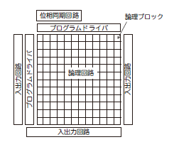
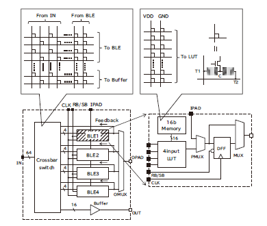
An NBFPGA consists of an array of logic blocks, input/output circuits that exchange logic signals with external components, program drivers to configure the NanoBridges, and a phase-locked loop (PLL) that generates the clock signal.
Each logic block contains four basic logic elements (BLEs) and a crossbar switch that determines the destination of logic signals. A BLE is composed of a Look-Up Table (LUT) for combinational logic and a D-type Flip-Flop (DFF) for
sequential logic. NanoBridges are used both in the crossbar switch and in the memory of the LUTs.
The crossbar switch is made up of NanoBridges. By turning on one NanoBridge in each row, the output destination of a logic block’s input signal is determined. The destination can be either a BLE or a neighboring logic block. Each LUT has 16 memory cells, and one value is selected and output based on the LUT input signal. The LUT memory is also composed of NanoBridges. By programming the NanoBridges in the crossbar switches and LUTs to be on or off, the circuit configuration is established, enabling user applications to run.
By using NanoBridges as memory elements in LUTs and as switches in the interconnects, the area of the logic blocks can be reduced. This leads to shorter wiring lengths, enabling higher speed and lower power consumption.
フィールドプログラマブルゲートアレイ(FPGA)は、内部回路(ハードウェア)をプログラムして、ユーザのアプリケーションに合わせて処理ブロックや処理フローを回路上に構築できる集積回路であり、CPUと同様に高い柔軟性を備えています。非ノイマン型のハードワイヤードロジック(布線論理)で情報処理を行うため、ノイマン型のプロセッサに比べて電力効率が高く、これまで以上に端末でのコンピューティングにおいて重要な役割を担っていくと考えられます。
課題: FPGAは汎用品であるため、ユーザが独自に集積回路を開発する必要がはありませんが、回路構成を変更するための半導体スイッチと回路構成を記憶する多量の半導体メモリ(SRAM)が搭載されているため、回路面積と待機電力が大きくなるという課題があります。さらにSRAMにおいては、情報の維持に電力が必要となるため、待機電力を消費しますし、揮発性メモリであるため頻繁に電源のオンオフをすることができません。
NBFPGA: NBFPGAは、アレイ状に配置された論理ブロック、外部と論理信号をやりとりする入出力回路、NanoBridgeをプログラムするためのプログラムドライバ、更にクロック信号を生成する位相同期回路から構成されています。論理ブロックは、4つの基本論理エレメント(BLE)、論理信号の接続先を決めるクロスバースイッチから構成されています。BLEは、組み合わせ論理演算が行われるルックアップテーブル(LUT)、順序論理演算が行われるDタイプフリップフロップ(DFF)から構成されており、NanoBridgeをクロスバースイッチとLUTのメモリに使用します。クロスバースイッチは、NanoBridgeから構成され、各行のいずれかのNanoBridgeをオンとすることによって、論理ブロックの入力信号の出力先が決まります。出力先は、BLEあるいは隣接する論理ブロックのいずれかが選ばれます。1つのLUTは16個のメモリを備えており、LUTの入力信号に従って選ばれた16個のメモリのうち1つの値が出力されます。LUTのメモリもNanoBridgeから構成されています。クロスバースイッチ及びLUTを構成するNanoBridgeをオンまたはオフにプログラムすることによって回路構成が決まり、ユーザーのアプリケーションが実行できます。このようにLUTのメモリや配線を切り替えるスイッチにNanoBridgeを用いることで、論理ブロックの面積を小さくでき、結果的に、配線長を短くすることによる高速化、及び低消費電力化を実現できます。
NBFPGA
NBFPGA architecture using NanoBridge